Apple's Huge 3nm Chip Orders for iPhone 15 Pro and M3 Macs Helping to Maintain TSMC's Fab Utilization Rates

Apple supplier TSMC is making strides to improve its production capacity for chips based on its cutting-edge 3-nanometer process technology, according to industry sources, which is expected to debut in this year's iPhone 15 Pro and upcoming MacBook models.

tsmc semiconductor chip inspection 678x452
DigiTimes reports that TSMC's 5nm fabrication capacity began to loosen in November 2022 as a result of reduced orders from Apple, amongst other partners, with orders for ‌iPhone‌ chips alone having been slashed by 30%. However, the Taiwanese manufacturer has apparently been able to keep its utilization rate at 70% or higher thanks to Apple's thirst for 3nm:

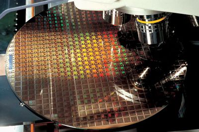
TSMC continues to improve its capacity utilization for 3nm process technology, which is expected to approach 50% at the end of March, the sources said. The foundry will also grow the process output to 50,000-55,000 wafers monthly in March, with Apple being the main customer.

Apple's upcoming ‌iPhone‌ 15 Pro models are expected to feature the A17 Bionic processor, Apple's first ‌iPhone‌ chip based on TSMC's first-generation ‌3nm‌ process, also known as N3E.

The first-gen ‌3nm‌ process is said to deliver a 35% power efficiency improvement over TSMC's 5nm-based N4 fabrication process, which was used to make the A16 Bionic chip for the ‌iPhone‌ 14 Pro and Pro Max. The N3 technology will also offer significantly improved performance compared to current chips manufactured on 5nm.

Apple's next-generation 13-inch and 15-inch MacBook Air models are both expected to be equipped with an M3 chip, which is also likely to be manufactured on the ‌3nm‌ process for further performance and power efficiency improvements. Apple is also reportedly planning to release an updated version of the 13-inch MacBook Pro with an M3 chip. The M2 chip and its higher-end Pro and Max variants are built on TSMC's second-generation 5nm process.

Orders for new AI processors from Nvidia and AMD, as well as Apple's new ‌iPhone‌ chip, are expected to help TSMC avoid further fab utilization declines in the second quarter, DigiTimes' sources said.

Popular Stories

Apple Logo Zoomed

Tim Cook Teases Plans for Apple's Upcoming 50th Anniversary

Thursday February 5, 2026 12:54 pm PST by
Apple turns 50 this year, and its CEO Tim Cook has promised to celebrate the milestone. The big day falls on April 1, 2026. "I've been unusually reflective lately about Apple because we have been working on what do we do to mark this moment," Cook told employees today, according to Bloomberg's Mark Gurman. "When you really stop and pause and think about the last 50 years, it makes your heart ...
wwdc sans text feature

Apple Rumored to Announce New Product on February 19

Thursday February 5, 2026 12:22 pm PST by
Apple plans to announce the iPhone 17e on Thursday, February 19, according to Macwelt, the German equivalent of Macworld. The report, citing industry sources, is available in English on Macworld. Apple announced the iPhone 16e on Wednesday, February 19 last year, so the iPhone 17e would be unveiled exactly one year later if this rumor is accurate. It is quite uncommon for Apple to unveil...
Finder Siri Feature

Why Apple's iOS 26.4 Siri Upgrade Will Be Bigger Than Originally Promised

Friday February 6, 2026 3:06 pm PST by
In the iOS 26.4 update that's coming this spring, Apple will introduce a new version of Siri that's going to overhaul how we interact with the personal assistant and what it's able to do. The iOS 26.4 version of Siri won't work like ChatGPT or Claude, but it will rely on large language models (LLMs) and has been updated from the ground up. Upgraded Architecture The next-generation...
iOS 26

iOS 26.3 and iOS 26.4 Will Add These New Features to Your iPhone

Tuesday February 3, 2026 7:47 am PST by
While the iOS 26.3 Release Candidate is now available ahead of a public release, the first iOS 26.4 beta is likely still at least a week away. Following beta testing, iOS 26.4 will likely be released to the general public in March or April. Below, we have recapped known or rumored iOS 26.3 and iOS 26.4 features so far. iOS 26.3 iPhone to Android Transfer Tool iOS 26.3 makes it easier...
iphone 17 pro dark blue 1

iPhone 18 Pro Max Rumored to Deliver Next-Level Battery Life

Friday February 6, 2026 5:14 am PST by
The iPhone 18 Pro Max will feature a bigger battery for continued best-in-class battery life, according to a known Weibo leaker. Citing supply chain information, the Weibo user known as "Digital Chat Station" said that the iPhone 18 Pro Max will have a battery capacity of 5,100 to 5,200 mAh. Combined with the efficiency improvements of the A20 Pro chip, made with TSMC's 2nm process, the...

Top Rated Comments

iAFC Avatar
38 months ago

The industry is moving from nm to Ångströms. The node after 2 nm will be 18 å for example.
I'll finally find a use for this key on my Finnish keyboard.
Score: 20 Votes (Like | Disagree)
jdb8167 Avatar
38 months ago

What is the actual transistor size? I haven't been following that closely these past few years.
From Wikipedia:

The term "5 nm" has no relation to any actual physical feature (such as gate length, metal pitch or gate pitch) of the transistors being 5 nanometers ('https://en.m.wikipedia.org/wiki/Nanometer') in size. According to the projections contained in the 2021 update of the International Roadmap for Devices and Systems ('https://en.m.wikipedia.org/wiki/International_Roadmap_for_Devices_and_Systems') published by IEEE Standards Association Industry Connection, a "5 nm node is expected to have a contacted gate pitch of 51 nanometers and a tightest metal pitch of 30 nanometers".[3] ('https://en.m.wikipedia.org/wiki/5_nm_process#cite_note-3') However, in real world commercial practice, "5 nm" is used primarily as a marketing term by individual microchip manufacturers to refer to a new, improved generation of silicon semiconductor chips in terms of increased transistor density (i.e. a higher degree of miniaturization), increased speed and reduced power consumption compared to the previous 7 nm process ('https://en.m.wikipedia.org/wiki/7_nm_process').
https://en.m.wikipedia.org/wiki/5_nm_process


The term "3 nanometer" has no relation to any actual physical feature (such as gate length, metal pitch or gate pitch) of the transistors. According to the projections contained in the 2021 update of the International Roadmap for Devices and Systems ('https://en.m.wikipedia.org/wiki/International_Roadmap_for_Devices_and_Systems')published by IEEE Standards Association Industry Connection, a 3 nm node is expected to have a contacted gate pitch of 48 nanometers and a tightest metal pitch of 24 nanometers.[14] ('https://en.m.wikipedia.org/wiki/3_nm_process#cite_note-14')However, in real world commercial practice, "3 nm" is used primarily as a marketing term by individual microchip manufacturers to refer to a new, improved generation of silicon semiconductor chips in terms of increased transistor density (i.e. a higher degree of miniaturization), increased speed and reduced power consumption.[15] ('https://en.m.wikipedia.org/wiki/3_nm_process#cite_note-15')[16] ('https://en.m.wikipedia.org/wiki/3_nm_process#cite_note-16') Moreover, there is no industry-wide agreement among different manufacturers about what numbers would define a 3 nm node. Typically the chip manufacturer refers to its own previous process node (in this case the 5 nm process ('https://en.m.wikipedia.org/wiki/5_nm_process')node) for comparison. For example, TSMC has stated that its 3 nm FinFET chips will reduce power consumption by 25-30% at the same speed, increase speed by 10-15% at the same amount of power and increase transistor density by about 33% compared to its previous 5 nm FinFET chips.[17] ('https://en.m.wikipedia.org/wiki/3_nm_process#cite_note-17')[18] ('https://en.m.wikipedia.org/wiki/3_nm_process#cite_note-18') On the other hand, Samsung has stated that its 3 nm process will reduce power consumption by 45%, improve performance by 23%, and decrease surface area by 16% compared to its previous 5 nm process.
https://en.m.wikipedia.org/wiki/3_nm_process
Score: 16 Votes (Like | Disagree)
Aston441 Avatar
38 months ago
3 nanometer circuits... I still find this amazing. The first processor I ever experimented with was at 3500 nm. Not a typo.
Score: 13 Votes (Like | Disagree)
Aston441 Avatar
38 months ago

From Wikipedia:


https://en.m.wikipedia.org/wiki/5_nm_process
Holy crap! It's marketing BS ?

I thought something was off. Years ago I remember reading that below 5nm might be impossible due to quantum effects / hard physical reality.

Obviously marketing doesn't have those limitations.
Score: 11 Votes (Like | Disagree)
User 6502 Avatar
38 months ago

3 nanometer circuits... I still find this amazing. The first processor I ever experimented with was at 3500 nm. Not a typo.
it doesn’t seem real because it isn’t. The whole nm thing largely lost meaning and it has little to do with the actual transistor size. Sure there has been huge progress and they can squeeze so many more transistors in the same area than they used to, but 3nm is a misleading number. The truth is that we got to the limit of what’s physically possible: silicon atoms have a size and you can’t change that fact no matter how much research you do.
Score: 9 Votes (Like | Disagree)
jdb8167 Avatar
38 months ago

Does anyone else see what’s happening here? Eventually the nm will require floating point numbers, and these devices will be in more everyday devices running chatGPT 10.0 and replace us (although I think 100-200 year timeline on that last part, if not 5000).
The industry is moving from nm to Ångströms. The node after 2 nm will be 18 å for example.
Score: 7 Votes (Like | Disagree)